|
A covered panel on which attached tour and elements such as microchips are attached or personalized.
Background
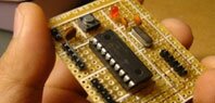
A printed out enterprise panel, or PCB, is a self-contained component of attached automated elements found in gadgets including common beepers, or pagers, and receivers to innovative mouth and pcs. The tour are established by a slim coating of performing materials placed, or "printed," on the exterior of an insulating material panel known as the substrate. Individual automated elements are placed on the exterior of the substrate and soldered to the adjacent tour. Get in touch with hands and fingers along one or more factors of the substrate act as associations to other PCBs or to exterior electric powered gadgets such as on-off changes. A printed out enterprise panel may have tour that perform 1 function, such as an indication firm, or several features.
There are three major kinds of printed out enterprise panel construction: single-sided, double-sided, and multi-layered. Single-sided forums have the elements on one aspect of the substrate. When the number of elements becomes too much for a single-sided panel, a double-sided panel may be used. Electro-mechanical associations between the tours on each aspect are created by exploration gaps through the substrate in appropriate places and plating the inside of the gaps with a performing material. The third type, a multi-layered panel, has a substrate created up of levels of printed out tour split up by levels of insulating material. The elements on the exterior are attached through coated gaps drilled down to the appropriate enterprise coating. This significantly makes easier the enterprise design.
Components on a printed out enterprise panel are electric attached to the tour by two different methods: the older "through pit technology" and the modern "surface install technological innovation." With through pit technological innovation, each element has slim wiring, or brings which are encouraged through little gaps in the substrate and soldered to network shields in the tour on lack of. Severity and scrubbing between brings and the edges of the gaps keep the elements in position until they are soldered. With exterior install technological innovation, stubby J-shaped or L-shaped feet on each element contact the printed out tour immediately. Two other kinds of enterprise devices are related to the printed out enterprise panel. An enterprise, sometimes called an IC or micro-chip, works similar features to a printed out enterprise panel except the IC contains many more tour and elements that are electrochemically "grown" in position on the exterior of a very little nick of plastic. A several enterprise, as the name indicates, looks like a printed out enterprise panel, but contains some elements that are produced onto the exterior of the substrate rather than being placed on the exterior and soldered.
|